


BSM Series Modular SWIR Microscope System
Product Introduction
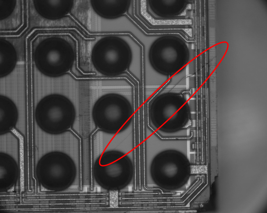
The BSM modular SWIR microscope system is a next-generation Short-Wave Infrared imaging platform that extends the imaging range from the traditional visible band (400-700 nm) to 900-1700 nm. By combining high-sensitivity InGaAs sensor technology with dedicated M Plan Apo NIR objectives, it breaks through the optical barrier of silicon-based materials to deliver non-destructive, through-silicon inspection. The modular architecture integrates advanced illumination, imaging, and precision mechanics, providing micrometre-level subsurface defect detection capabilities for semiconductor manufacturing, materials science, and industrial inspection. Standard glass optics eliminate the need for costly reflective components, significantly lowering the technical barrier and overall cost for SWIR imaging.
Product Features
- Full coverage of the 900-1700 nm SWIR imaging band
- Penetrating imaging through silicon-based materials for non-destructive internal inspection
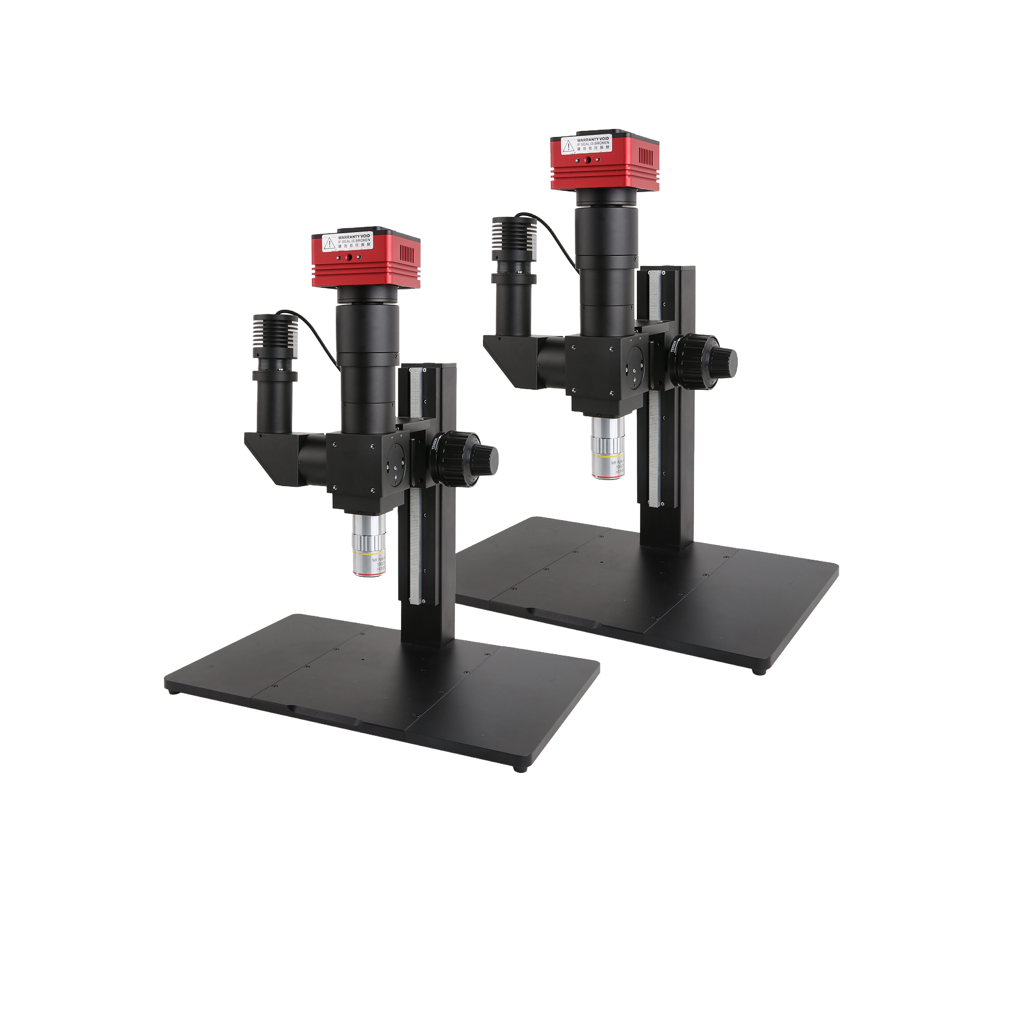
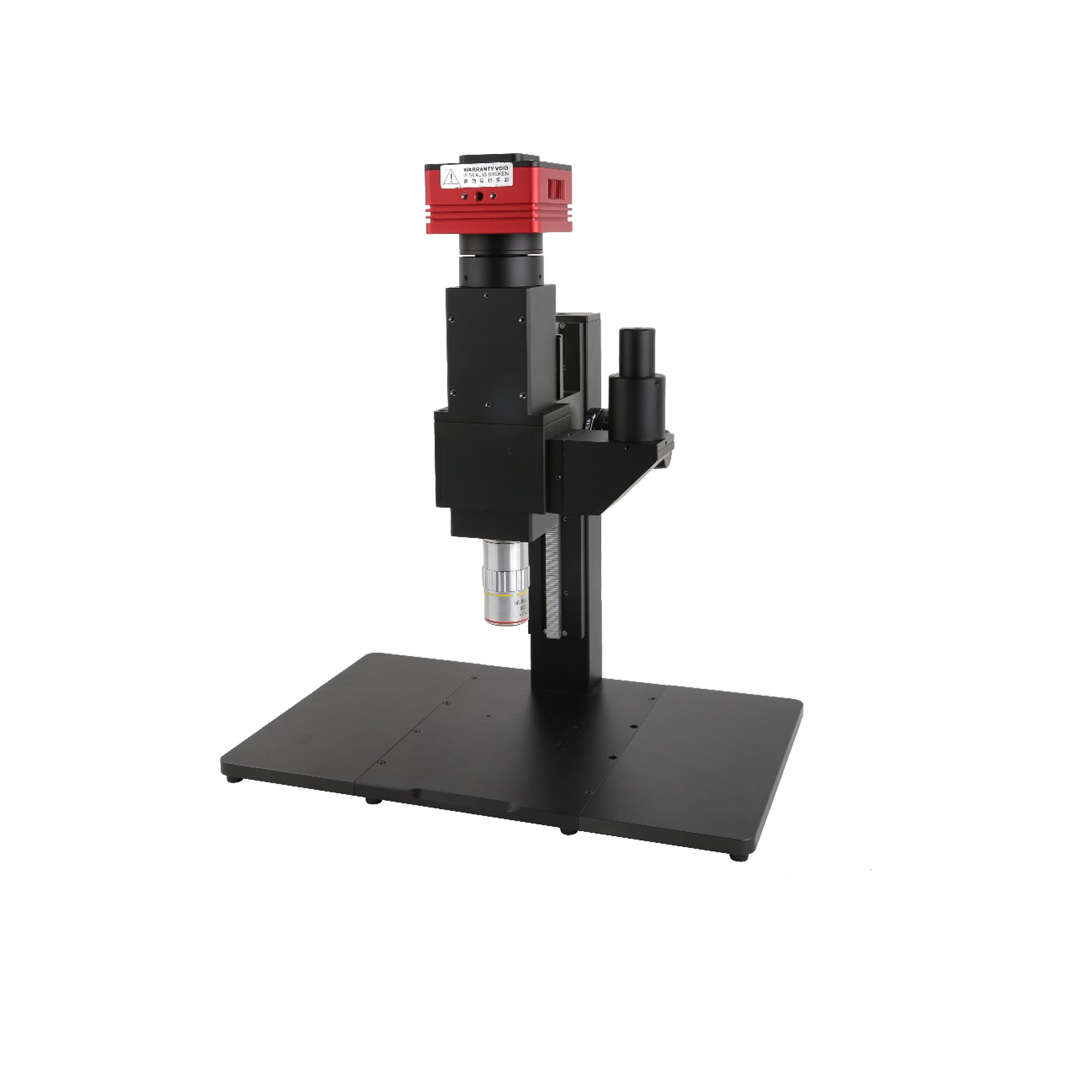
- Three tube-lens systems available (BSM-T180VA / T090VA / T100VA)
- Image circle up to 33 mm to support large-format sensors
- M Plan Apo NIR objective range (5X-50X HR)
- 0.4 µm ultra-high optical resolution (50X HR objective)
- Coaxial epi-illumination Köhler lighting system
- Integrated LED sources at 1200 / 1300 / 1400 / 1550 nm
- Compatible with high-performance InGaAs cameras (0.33 MP-5.0 MP)
- Real-time imaging up to 400 fps@640×512
- TEC cooling ensures low-noise, high-SNR imaging
- Standard C-mount interface for broad camera compatibility
- Modular architecture supporting flexible customisation and upgrades
- Precision CNC machining with anti-vibration design
- Standard glass optics for optimised cost-effectiveness
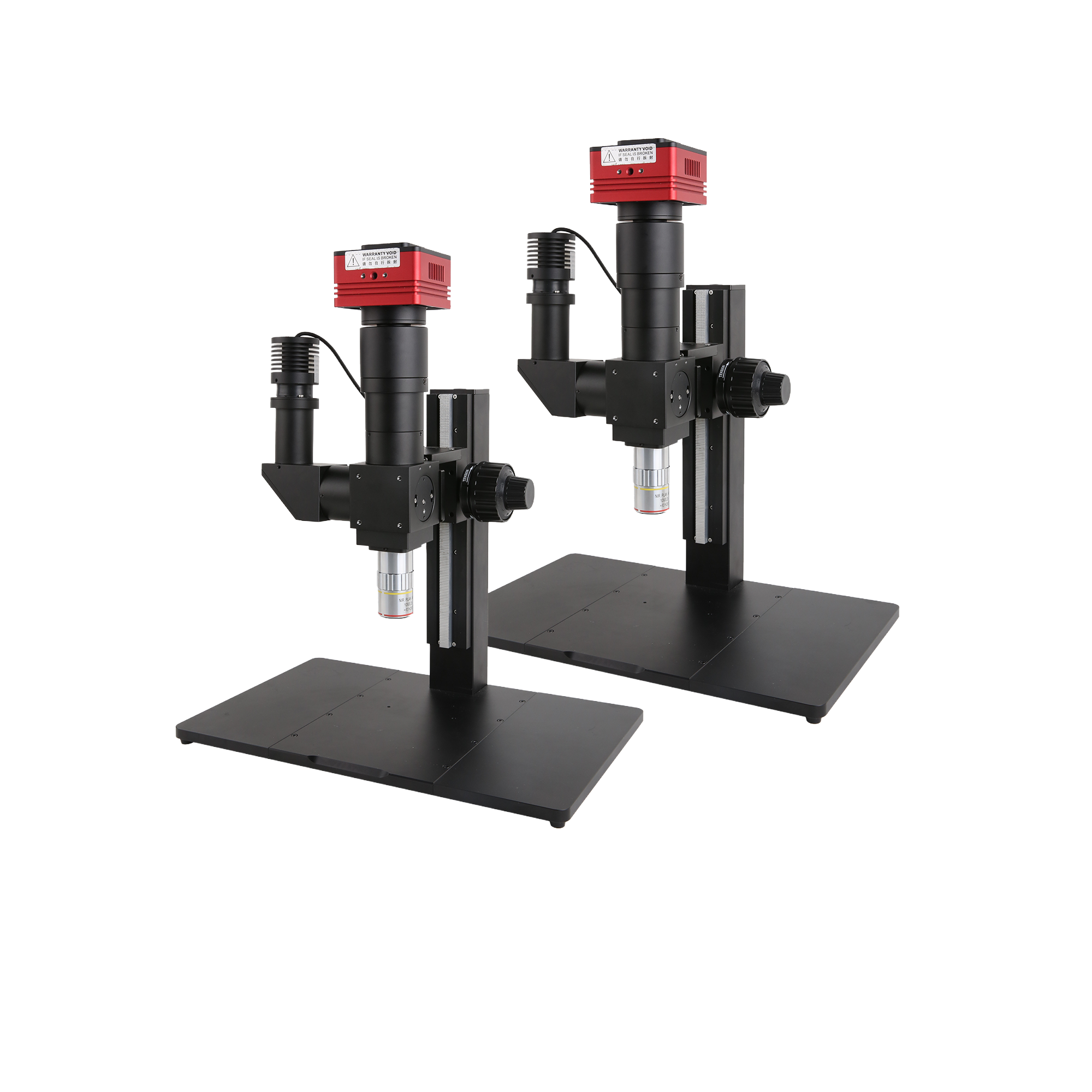
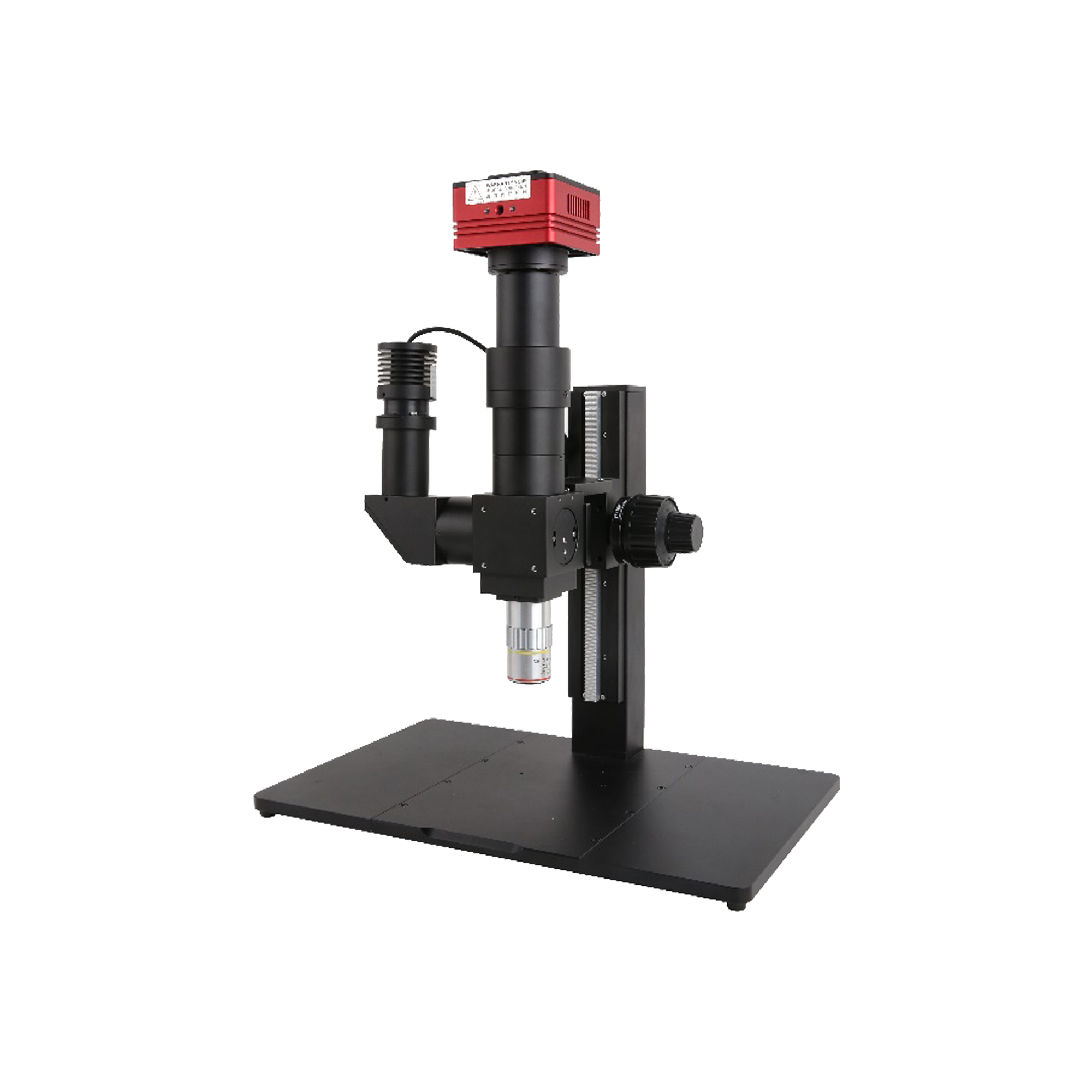
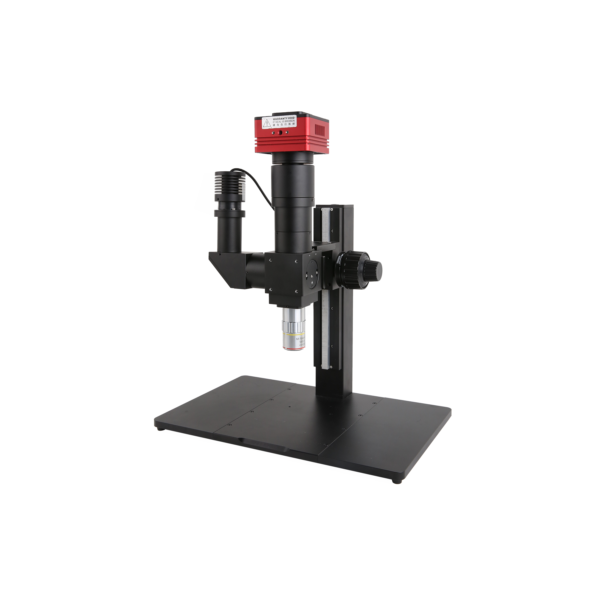
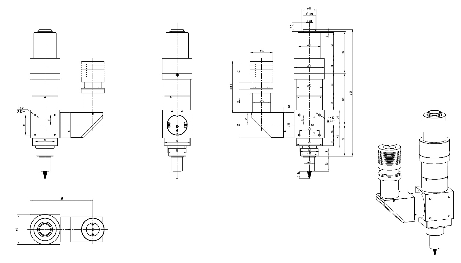
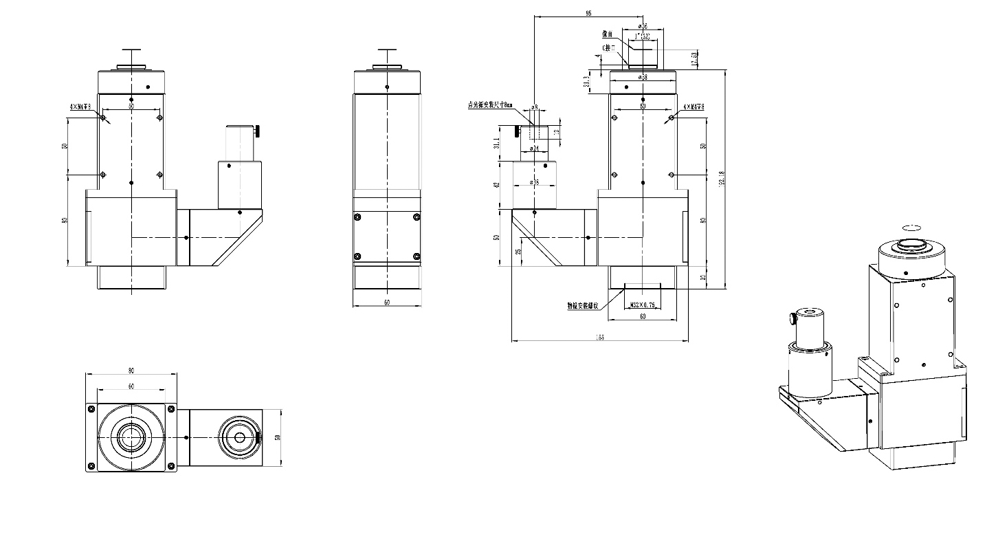
System Configuration and Parameters
SWIR microscopy imaging technology breaking traditional optical limitations, providing revolutionary solutions for semiconductor and material inspection
System Technical Principle
The BSM series exploits the unique physical characteristics of SWIR light to perform through-silicon imaging of silicon-based and other semiconductor materials. Precision optical design combined with high-sensitivity sensors reveals internal structures that conventional microscopes cannot observe.
Silicon Penetration Imaging
SWIR photons have lower energy than the silicon bandgap (1.1 eV), enabling through-silicon imaging for non-destructive inspection of subsurface defects such as micro-cracks and solder faults
Optical Compatibility
Uses standard glass optics, avoiding the expensive reflective components required for mid- and long-wave infrared imaging, which lowers production cost and simplifies system integration
Modular Architecture
Illumination, imaging, and mechanical modules are independently designed, supporting custom upgrades for specific wavelengths, sensors, or automation needs
Enhanced Material Contrast
SWIR wavelengths improve the visibility of features obscured in the visible band, allowing clear imaging of internal structures in composite materials
Tube Lens System Configuration
Standard Configuration – Universal Inspection Platform
Model: BSM-T180VA / BSM-T090VA
- Tube Lens Focal Length
- 180 mm / 90 mm
- Image Field Size
- 24 mm (180 mm tube lens)
- Spectral Range
- 900-1700 nm
- Illumination Method
- Coaxial epi-illumination Köhler
- LED Light Sources
- 1200/1300/1400/1550 nm
High-End Configuration – Maximum Performance Platform
Model: BSM-T100VA
- Tube Lens Focal Length
- 100 mm
- Image Field Size
- 33 mm (200 mm tube lens)
- Spectral Range
- 900-1700 nm
- Illumination Method
- Coaxial epi-illumination Köhler
- LED Light Sources
- 1200/1300/1400/1550 nm
M Plan Apo NIR Objective Series
High-performance microscope objectives optimised for the SWIR band, delivering outstanding image quality and penetration capability
| Model | Magnification | NA | WD | Focal Length | Resolution | Depth of Field | FN | Weight |
|---|---|---|---|---|---|---|---|---|
| M Plan Apo NIR 5X | 5X | 0.14 | 37.5 mm | 40 mm | 2.0 µm | 14 µm | 24 mm | 220 g |
| M Plan Apo NIR 10X | 10X | 0.26 | 30.5 mm | 20 mm | 1.1µm | 4.1 µm | 24 mm | 250 g |
| M Plan Apo NIR 20X | 20X | 0.4 | 20 mm | 10 mm | 0.7µm | 1.7 µm | 24 mm | 300 g |
| M Plan Apo NIR 50X | 50X | 0.42 | 17 mm | 4 mm | 0.7µm | 1.6 µm | 24 mm | 315 g |
|
M Plan Apo NIR 50X HR High-resolution version |
50X | 0.65 | 10 mm | 4 mm | 0.4 µm | 0.7µm | 24 mm | 450 g |
SWIR Camera Lineup
High-performance InGaAs cameras with TEC cooling deliver outstanding signal-to-noise ratio and image quality
SWIR5000KMA
- Sensor
- 5.0 MP IMX992 (M, GS)
- Sensor Size
- 1/1.4'' (8.94×7.09 mm)
- Pixel Size
- 3.45×3.45 µm
- SNR
-
High Gain: 51.5 dB
Low Gain: 48.5 dB - Frame Rate
-
61.9@2560×2048
135.7@1280×1024 - Exposure Time
- 15 µs~60 s
- Cooling
- Built-in TEC
SWIR3000KMA
- Sensor
- 3.0 MP IMX993 (M, GS)
- Sensor Size
- 1/1.8'' (7.07×5.3 mm)
- Pixel Size
- 3.45×3.45 µm
- SNR
-
High Gain: 51.5 dB
Low Gain: 48.5 dB - Frame Rate
-
93@2048×1536
176@1024×768 - Exposure Time
- 15 µs~60 s
- Cooling
- Built-in TEC
SWIR1300KMA
- Sensor
- 1.3 MP IMX990 (M, GS)
- Sensor Size
- 1/2'' (6.40×5.12 mm)
- Pixel Size
- 5×5 µm
- SNR
-
High Gain: 58.7 dB
Low Gain: 52.6 dB - Frame Rate
-
200@1280×1024
392@640×512 - Exposure Time
- 15 µs~60 s
- Cooling
- Built-in TEC
SWIR330KMA
- Sensor
- 0.33 MP IMX991 (M, GS)
- Sensor Size
- 1/4'' (3.20×2.56 mm)
- Pixel Size
- 5×5 µm
- SNR
-
High Gain: 58.7 dB
Low Gain: 52.6 dB - Frame Rate
-
400@640×512
753@320×256 - Exposure Time
- 15 µs~60 s
- Cooling
- Built-in TEC
Typical Application Cases
Professional applications of BSM system in semiconductor manufacturing, materials science, and other fields
Semiconductor manufacturing and inspection
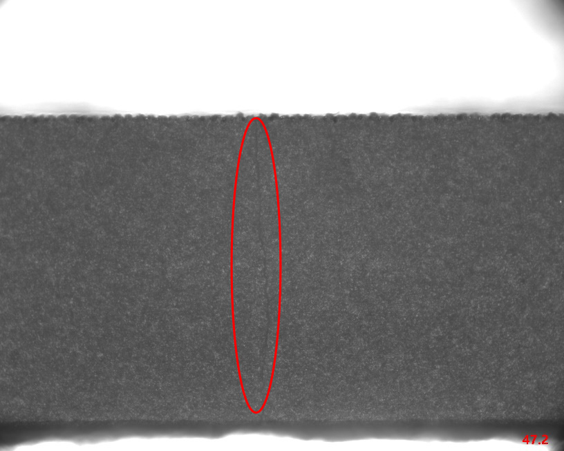
During semiconductor manufacturing, the BSM series performs non-destructive inspection of silicon wafers and chips. It penetrates silicon-based materials to reveal subsurface defects, micro-cracks, and interconnect structures, supporting quality control and failure analysis.
Application Case
- Non-destructive inspection of defects inside silicon wafers
- Evaluation of chip interconnect integrity
- Precise localisation of subsurface micro-cracks
- Real-time monitoring of welding quality
- Package integrity verification
Ceramic material defect inspection
The system plays a critical role in ceramic and composite inspection, identifying subsurface cracks, pores, and inclusions. SWIR imaging exposes internal defects invisible to conventional optics, providing reliable data for material quality assessment.
Application Case
- Visualisation of internal cracks in ceramics
- Layer inspection of composite materials
- Pore distribution analysis
- Identification and localisation of inclusions
- Structural integrity assessment
More Application Fields
Industrial non-destructive testing
The BSM series delivers high-precision, non-destructive inspection for industrial components. It visualises internal structures, detects assembly defects, and evaluates material uniformity without dismantling the product, enabling comprehensive quality assessment.
- Component internal structure analysis
- Assembly quality verification
- Material uniformity evaluation
Materials science research
In materials science research, the system analyses new materials' microstructures, phase distributions, and defect characteristics. SWIR imaging offers distinctive contrast, helping correlate material performance with microstructure.
- Structural characterisation of new materials
- Phase distribution visualisation
- Grain boundary observation and analysis
Technology Advantages Comparison
| Comparison Technology | BSM System Advantages |
|---|---|
| Conventional optical microscopes | BSM systems penetrate silicon and other opaque materials to reveal internal structures, whereas conventional microscopes are limited to surface observation |
| X-ray inspection | BSM provides higher resolution, no radiation hazard, real-time imaging, and lower equipment and maintenance costs |
| Ultrasonic inspection | BSM delivers higher spatial resolution and image clarity, identifying micrometre-scale defects |
| Mid-wave / long-wave infrared systems | BSM uses standard glass optics for lower cost and better compatibility with existing microscope platforms |
System Configuration and Accessories
Standard Configuration
- BSM main system (choice of T180VA / T090VA / T100VA)
- Multi-wavelength LED illumination module
- Coaxial epi-illumination system
- C-mount camera adapter
- Precision focusing mechanism
Optional Accessories
- M Plan Apo NIR objective range (5X-50X HR)
- SWIR camera series (330K-5000K resolution)
- Automated sample stage
- Image acquisition and analysis software
- Anti-vibration platform
- Custom-wavelength LED light sources
The BSM Series features modular architecture design, supporting customized upgrades based on specific wavelength, sensor, or automation requirements
BSM System Advantages
Revolutionary SWIR microscopy imaging technology, opening a new era of material internal inspection
Silicon Penetration Imaging Capability
SWIR photon energy is below the silicon band gap, enabling non-destructive detection of internal defects in silicon-based materials, including micro-cracks, solder failures, and other subsurface defects.
Wide-Band Imaging Coverage
900-1700 nm wide-band imaging capability with multi-wavelength LED light sources, meeting imaging requirements for different materials and applications.
Modular Architecture Design
Independent design of illumination, imaging, and mechanical modules, supporting customized upgrades based on specific requirements, ensuring system flexibility and expandability.
Cost-Effective Solution
Uses standard glass optical elements, avoiding expensive reflective optical systems, reducing equipment costs and maintenance fees.
Real-Time Imaging Capability
High-speed InGaAs sensors support real-time imaging with frame rates up to 400 fps, meeting online inspection and dynamic observation requirements.
Micron-Level Resolution
Professional M Plan Apo NIR objective series achieves resolution up to 0.4 µm, precisely identifying minute defects and structural details.